- About
- My Account
- Contact
- Get A Quote: 1 800 496 9918
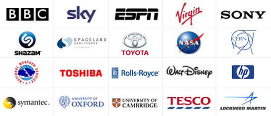
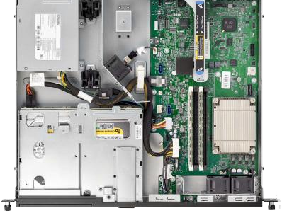
 HPE ProLiant DL360 Gen10
The HPE ProLiant DL360 Gen10 Server delivers security, agility and flexibility without compromise.
 HPE ProLiant DL380 Gen10
The HPE ProLiant DL380 Gen10 Server is securely designed to reduce costs and complexity.
 HPE ProLiant DL385 Gen10 Plus
The HPE ProLiant DL385 Gen10 Server redefines price/performance for virtualisation.
 HPE ProLiant ML350 Gen10
The HPE ProLiant ML350 Gen10 delivers the ideal levels of performance and expandability
 HPE ProLiant DL360 Gen10 Plus
The HPE ProLiant DL360 Gen10 Plus Server delivers enhanced performance over the previous generation.
 HPE ProLiant DL380 Gen10 Plus
The HPE ProLiant DL380 Gen10 Plus Server introduces the latest 3rd Gen Intel Xeon Scalable processor.
HPE ProLiant DL385 Gen10 Plus V2
The HPE ProLiant DL385 Gen10 Plus V2 Server introduces the latest AMD EPYC Gen 3 processor
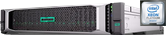
 HPE MSA 2060
Cost-effective, high performance systems that deliver speed, scalability and efficiency in a dense design.
HPE MSA 2052
Seriously simple and affordable flash storage designed for affordable application acceleration.
HPE MSA 2050
Affordable, high-performance shared storage designed for affordable application acceleration.
HPE MSA 1050
Affordable, high-performance shared storage designed for affordable application acceleration.
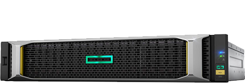
 HPE StoreEasy 3850 Gateway
The right balance of performance, storage, reliability, manageability and efficiency in a dense and compact chassis
ServerWarehouse boasts the world's best HPE server configurator. Build your HPE server today.
Our advanced server configurator allows over a million possible server configurations!
Every month, 100,000+ users configure their ideal HPE solution online & get an instant quote!
ServerWarehouse supply all of the top 20 universities the US with configured HPE server and storage solutions.

 Extensive Testing
Before leaving our build and configuration facility, all of our server and storage solutions undergo an extensive 48 hour testing procedure. This, along with OEM HPE components we use ensure all of our server and storage solutions meet the strictest quality guidelines demanded from us.
 Customization Service
Our main objective is to offer great value, high quality server and storage solutions, we understand that every company has different requirements and as such are able to offer a complete customization service to provide server and storage solutions that meet your individual needs.
We have established ourselves as one of the biggest storage providers in the US, and since 1989 been trusted as the preferred supplier of server and storage solutions to some of the world's biggest brands, including: